
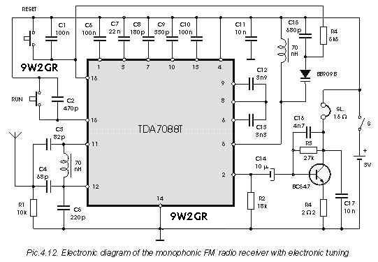
The electronic diagram of the monophonic FM receiver made with TDA7088T is shown on Pic.4.12. If built with SMD components it can be placed in a matchbox, altogether with two button-type batteries. The operating principle of this device is given in the previous chapter. The only thing new is a very simple audio amplifier made with BC547 transistor, which is loaded by cheap 16-Ohm headphones. The telescopic antenna is used, as on Pic.4.8. Small mishap of this receiver is that it has no indication of station tuning. This problem can be solved by adding a small voltmeter in parallel to the BB909, whose scale is graduated in MHz, as described in the Appendix. This solution is not appropriate for the miniature receiver, since the voltmeter that has the scale that is big enough takes too much space. It is in this case better using a manual tuning instead of automatic. Such solution is given on Pic.4.13. The tuning is done via the variable capacitor C with numbers written on its button, similar to that on Pic.3.11. It is most simple to use numbers from 1 to 10. The variable capacitor is like the one on Pic.4.8. Some experimenting is to be done with capacitances of Cx and Cy, in order to cover the entire reception bandwidth, from 88 till 108 MHz.


The AFC (Automatic Frequency Control) of the local oscillator is accomplished with BA483 diode, obtaining that station's position on scale does not "walk" over the scale. The complete radio receiver should still have a loudspeaker. Electronic diagram of such receiver made with TDA7088T is given on Pic.4.14. As one can see, that is a receiver from Pic.4.12 with an audio receiver made with LM386 IC. Maximum value of the DC supply voltage for the TDA7088T is 5V, therefore if using a 4.5 V battery the LM386 will work with reduced output power, the D2 diode and C15 capacitor should be omitted, and R4 should be short-circuited.
If higher voltage battery is used, the voltage stabilizer, comprised by the aforementioned components, has to be activated. D2 is a Zener diode with 3 V Zener voltage. The optimum value of R4 is found experimentally: in order to make the power consumption as low as possible it should have the resistance as big as possible, while simultaneously keeping the voltage on Pin 4 about 3 V and the device working well within the entire reception bandwidth (One should start with, say, R4=1.5 kOhm, and if the receiver operates well bigger resistance should be tried out, and if not smaller one, until the optimum value is found).
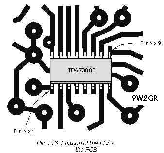
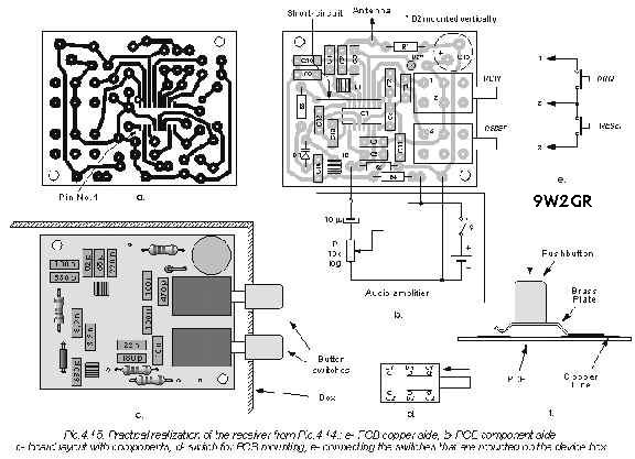
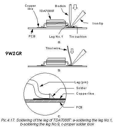
Pic.4.15. shows the PCB for the HF part of the receiver with TDA7088T, that is realized with ordinary components, instead of the SMD's. Pic.4.15-a shows the board layout from the soldering (copper) side. All the components apart from TDA7088T are mounted on the opposite side of the board, their pins are put through the holes and soldered through the holes. The TDA is soldered on the copper side, directly onto the copper contacts. That is why it is being drawn in dashed line on pic.4.15-b, where the board layout on the component side is given. * Pic.4.16-a shows 3x enlarged picture of the IC and the surrounding lines. The soldering procedure for SMD is as follows: A thin tin layer is applied on the copper contacts where IC legs are to be soldered to. The firs legs to be soldered are the diagonally opposite ones, in this case No.1 and 9. A small cushion-shaped amount of tin (not profuse) is applied on the contacts where these pins are to be soldered (pic.4.17-a). The IC is placed in its position, with all the pins properly laid. Pin No.1 is pressed against the tin pillow with a top of a bodkin, with iron head simultaneously touching both the tin and the pin end. The tin gets melted, and the pin lies down on its place with the aid of the bodkin, and gets soldered. It is now time to check out the positioning of the chip. If it needs to be corrected, the tin surrounding the pin No.1 is melted with iron tip and the chip position is quickly and carefully adjusted, in order not to overheat the pin. Soldering the pin No.9 is shown on Pic.4.17-b. First, the iron tip is simultaneously put on the top of the leg and the copper below it, so that both of them are heated. After app. half a second, the iron is slightly removed from the leg but remains on the copper contact. The tip of the tinol wire is then approached to touch the iron, the pin top and the copper contact at the same time. The wire gets melted and adheres to the copper and the pin, so it has to be constantly moved downwards. When enough tin is applied, the tinol wire is removed first, then the iron, and the pin No.9 is soldered. Once again you have to check whether all the pins are properly placed, and then they too are soldered as it was just described. The solders are OK if they look app. as on Pic.4.17-c.
* Pic.4.15-b contains the PCB component side layout. The pushbuttons we used here are Siemens, type BO2AMAP-2. The common housing contains, as one can see, two button switches, one of which is being used by this device. Any other pushbutton switches can also be used. In that case small modifications on the PCB lines would probably be necessary. The board is mounted fairly close to the box edge, so that the switch shafts are passing through the panel, and that the buttons can be mounted on the outside. The panel-mount switches can also be used, in which case they are connected to the board by wires (pic.4.15-e).
* Any audio amplifier described so far can be used, e.g. the one with LM386, as on pic.4.8.
* Instead of the antenna, a 20 cm piece of wire can also be utilized.
[ Homebrew ] [ Homepage Utama ]